- 您现在的位置:买卖IC网 > Sheet目录1992 > CYW150OXC (Silicon Laboratories Inc)IC CLOCK 440BX AGP 56SSOP
CYW150
........................ Document #: 38-07177 Rev. *B Page 2 of 14
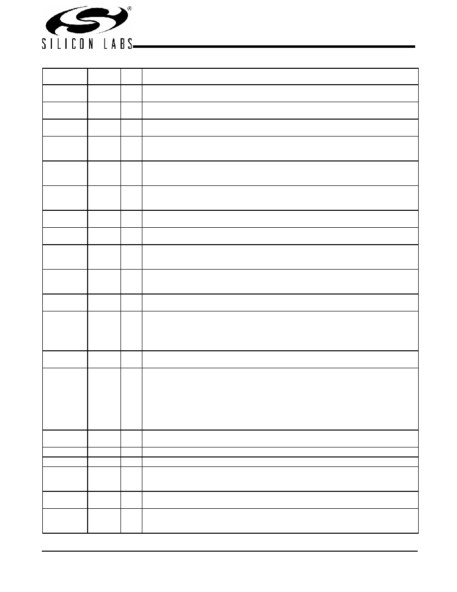
Pin Definitions
Pin Name
Pin No.
Pin
Type
Pin Description
CPU1:2
51, 49
O
CPU Outputs 1 and 2: Frequency is set by the FS0:3 inputs or through serial input interface,
CPU_F
52
O
Free-Running CPU Output: Frequency is set by the FS0:3 inputs or through serial input
PCI1:5
11, 12, 13,
14, 16
O
PCI Outputs 1 through 5: Frequency is set by the FS0:3 inputs or through serial input
PCI0/FS3
9
I/O
PCI Output/Frequency Select Input: As an output, frequency is set by the FS0:3 inputs or
PCI_STOP# input. When an input, latches data selecting the frequency of the CPU and PCI outputs.
PCI_F/MODE
8
I/O
Free Running PCI Output: Frequency is set by the FS0:3 inputs or through serial input
an input, selects function of pin 3 as described in Table 1.
CLK_STOP#
47
I
CLK_STOP# Input: When brought LOW, affected outputs are stopped LOW after completing
a full clock cycle (2–3 CPU clock latency). When brought HIGH, affected outputs start
beginning with a full clock cycle (2–3 CPU clock latency).
IOAPIC_F
54
O
Free-running IOAPIC Output: This output is a buffered version of the reference input which
is not affected by the CPU_STOP# logic input. Its swing is set by voltage applied to VDDQ2.
IOAPIC0
55
O
IOAPIC Output: Provides 14.318 MHz fixed frequency. The output voltage swing is set by
voltage applied to VDDQ2. This output is disabled when CLK_STOP# is set LOW.
48MHz/FS1
29
I/O
48 MHz Output: 48 MHz is provided in normal operation. In standard systems, this output can
be used as the reference for the Universal Serial Bus. Upon power up, FS1 input will be
latched, setting output frequencies as described in Table 2.
24MHz/FS0
30
I/O
24 MHz Output: 24 MHz is provided in normal operation. In standard systems, this output can
be used as the clock input for a Super I/O chip. Upon power up, FS0 input will be latched,
setting output frequencies as described in Table 2.
REF1/FS2
2
I/O
Reference Output: 14.318 MHz is provided in normal operation. Upon power-up, FS2 input
will be latched, setting output frequencies as described in Table 2.
REF0
(PCI_STOP#)
3I/O
Fixed 14.318 MHz Output 0 or PCI_STOP# Pin: Function determined by MODE pin. The
PCI_STOP# input enables the PCI 0:5 outputs when HIGH and causes them to remain at logic
0 when LOW. The PCI_STOP signal is latched on the rising edge of PCI_F. Its effects take
place on the next PCI_F clock cycle. As an output, this pin provides a fixed clock signal equal
in frequency to the reference signal provided at the X1/X2 pins (14.318 MHz).
SDRAMIN
17
I
Buffered Input Pin: The signal provided to this input pin is buffered to 17 outputs
(SDRAM0:15, SDRAM_F).
SDRAM0:15
44, 43,
41, 40,
39, 38,
36, 35,
22, 21,
19, 18,
33, 32,
25, 24
O
Buffered Outputs: These sixteen dedicated outputs provide copies of the signal provided at
the SDRAMIN input. The swing is set by VDDQ3, and they are deactivated when CLK_STOP#
input is set LOW.
SDRAM_F
46
O
Free-Running Buffered Output: This output provides a single copy of the SDRAMIN input.
The swing is set by VDDQ3; this signal is unaffected by the CLK_STOP# input.
SCLK
28
I
Clock pin for SMBus circuitry.
SDATA
27
I/O
Data pin for SMBus circuitry.
X1
5
I
Crystal Connection or External Reference Frequency Input: This pin has dual functions.
It can be used as an external 14.318 MHz crystal connection or as an external reference
frequency input.
X2
6
I
Crystal Connection: An input connection for an external 14.318-MHz crystal. If using an
external reference, this pin must be left unconnected.
VDDQ3
1, 7, 15,
20, 31,
37, 45
P
Power Connection: Power supply for core logic, PLL circuitry, SDRAM output buffers, PCI
output buffers, reference output buffers, and 48 MHz/24 MHz output buffers. Connect to 3.3V.
发布紧急采购,3分钟左右您将得到回复。
相关PDF资料
CYW173SXC
IC CLK GEN TAPE DRV 4CH 16SOIC
CYW305OXC
IC CLOCK W305 SOLANO 56SSOP
DAC5674IPHPG4
IC DAC 14BIT 400MSPS 48-HTQFP
DAC7621EBG4
IC SNGL 12BIT PARALLEL D/A 20SSO
DAC7801KPG4
IC DUAL 12BIT CMOS DAC 24-DIP
DAC8043AESZ
IC DAC 12BIT MULT SRL INP 8SOIC
DAC8043GP
IC DAC 12BIT MULTIPLY CMOS 8-DIP
DAC8221GP
IC DAC 12BIT DUAL W/BUFF 24-DIP
相关代理商/技术参数
CYW150OXCT
功能描述:时钟发生器及支持产品 Legacy-440BX AGP Refer to W150 DS RoHS:否 制造商:Silicon Labs 类型:Clock Generators 最大输入频率:14.318 MHz 最大输出频率:166 MHz 输出端数量:16 占空比 - 最大:55 % 工作电源电压:3.3 V 工作电源电流:1 mA 最大工作温度:+ 85 C 安装风格:SMD/SMT 封装 / 箱体:QFN-56
CYW152-12G
制造商:Rochester Electronics LLC 功能描述:- Bulk
CYW15G0101DXB
制造商:CYPRESS 制造商全称:Cypress Semiconductor 功能描述:Single-channel HOTLink II⑩ Transceiver
CYW15G0101DXB-BBC
功能描述:电信线路管理 IC Sngl Ch XCVR COM RoHS:否 制造商:STMicroelectronics 产品:PHY 接口类型:UART 电源电压-最大:18 V 电源电压-最小:8 V 电源电流:30 mA 最大工作温度:+ 85 C 最小工作温度:- 40 C 安装风格:SMD/SMT 封装 / 箱体:VFQFPN-48 封装:Tray
CYW15G0101DXB-BBI
功能描述:电信线路管理 IC Sngl Ch XCVR IND RoHS:否 制造商:STMicroelectronics 产品:PHY 接口类型:UART 电源电压-最大:18 V 电源电压-最小:8 V 电源电流:30 mA 最大工作温度:+ 85 C 最小工作温度:- 40 C 安装风格:SMD/SMT 封装 / 箱体:VFQFPN-48 封装:Tray
CYW15G0101DXB-BBXC
制造商:CYPRESS 制造商全称:Cypress Semiconductor 功能描述:Single-channel HOTLink II⑩ Transceiver
CYW15G0101DXB-BBXI
功能描述:电信线路管理 IC HOTLink II 1.5Gbps Single Channel RoHS:否 制造商:STMicroelectronics 产品:PHY 接口类型:UART 电源电压-最大:18 V 电源电压-最小:8 V 电源电流:30 mA 最大工作温度:+ 85 C 最小工作温度:- 40 C 安装风格:SMD/SMT 封装 / 箱体:VFQFPN-48 封装:Tray
CYW15G0201DXB
制造商:CYPRESS 制造商全称:Cypress Semiconductor 功能描述:Dual-channel HOTLink II⑩ Transceiver